PCB via capacitance
QuickField simulation example
Problem Type electrostatics.
Geometry 3D extrusion
Given
Relative permittivity of dielectric (FR-4) ε = 4.7;
Strip conductor potential V = 1 V.
Task
Calculate the printed circuit board via capacitance.
Solution
Capacitance can be calculated as C = 2·W / V², where W is the electric field energy, V - potential difference.
In 3D problem there is no way to separate the strip electric field from the via electric field. Therefore the total energy is calculated and the resulting capacitance is of the via + strip together.
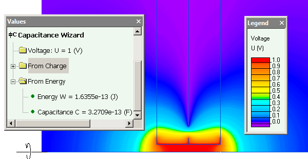
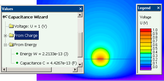
The 3D problem could be reduced to two 2D problems to calculate the via capacitance and strip conductor capacitance separately.
Results
Electric potential distribution in the dielectric board (click to view 3D picture):
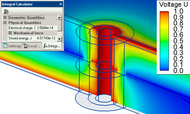
Electric field energy (3D problem) W = 4.0e-13 J
Via and strip combined capacitance
C = 2*4.0e-13 / 1² = 8e-13 F (0.80 pF).
Via and strip capacitance calculated as a sum of two values form 2D simulations is 0.77 pF, including:
- Video: PCB via capacitance. Watch on YouTube
- View simulation report in PDF
- Download simulation files (files may be viewed using any QuickField Edition).